
Mastering Precision in Thin Film Deposition: The Ultimate Guide to EQ-TM106 Thin Film Deposition Monitors
2026-06-18 09:33In the realm of advanced material science, the difference between a breakthrough and a failed experiment often lies in a few atomic layers. Whether you are working on Organic Light-Emitting Diodes (OLEDs), high-precision optical coatings, or next-generation semiconductor devices, the ability to monitor film growth in real-time is not just a luxury—it is a technical necessity.
Frequency Drift and Thermal Noise:
In thermal evaporation or sputtering, the environment inside the vacuum chamber is extremely hot. High temperatures cause the quartz crystal to expand, which changes its frequency independent of the deposited mass. This is known as "thermal drift."
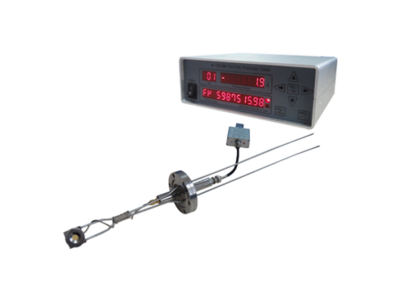
The EQ-TM106 thin film deposition monitor solution:
The EQ-TM106 utilizes advanced temperature-compensation algorithms. When paired with a water-cooled sensor head, it effectively filters out the noise generated by heat radiation, ensuring that the thickness reading you see is purely from material deposition, not thermal fluctuations.
Short Sensor Life and Sudden "Crystal Failure":
Nothing is more frustrating than a crystal failing in the middle of a 2-hour deposition process. Crystals typically fail due to "stress saturation" when the deposited film becomes too thick or begins to peel.
The EQ-TM106 thin film deposition monitor solution:
The device features a sophisticated Crystal Quality Indicator. It doesn't just tell you the thickness; it monitors the health of the crystal's oscillation. By providing a "Life %" or "Quality Factor," it allows researchers to replace the crystal before an experiment starts, preventing costly downtime and lost materials.
Complex Integration and Data Logging
Many older monitors use outdated serial ports or require proprietary, expensive software that is difficult to install on modern Windows 10/11 systems.
The EQ-TM106 thin film deposition monitor solution:
Designed for the modern lab, the EQ-TM106 features a plug-and-play USB interface. It comes with intuitive PC software that provides real-time graphing of both deposition rate and total thickness. This data can be exported directly to Excel or CSV for inclusion in research papers.
Step-by-Step Guide: Optimizing Your Deposition Process.
To get the most out of your EQ-TM106, follow these industry best practices for sensor setup:
Step 1: Geometry and Tooling Factor
The sensor cannot be placed exactly where your substrate is. Therefore, the thickness on the crystal might be slightly different from the thickness on your sample.
Tip: Perform a calibration run. Measure the actual film on your substrate using an AFM (Atomic Force Microscope) or Stylus Profiler, then adjust the Tooling Factor in the EQ-TM106 software to match the results.
Step 2: Crystal Selection
Gold Electrodes: Best for low-stress materials and general thermal evaporation.
Silver Electrodes: Preferred for high-rate processes due to better thermal conductivity.
Alloy Electrodes: Ideal for high-stress films like Chrome or Nickel.
Step 3: Maintaining the Vacuum Seal
The EQ-TM106 sensor head uses a KF40 or CF35 feedthrough. Always ensure the O-rings are lightly lubricated with vacuum-grade grease (like Krytox) to prevent micro-leaks that can destabilize the QCM signal.
Applications: Where the EQ-TM106 thin film deposition monitor excels.
Semiconductor Research
In the fabrication of transistors, gate oxide thickness must be controlled to within a few nanometers. The EQ-TM106 provides the precision needed for Al2O3 or HfO2 deposition.
Optical Coatings
Anti-reflective (AR) coatings rely on destructive interference, which requires layers to be exactly 1/4 the wavelength of light. The EQ-TM106’s 0.1 Å resolution makes it possible to hit these targets consistently.
Perovskite Solar Cells
Research into thin-film photovoltaics requires the deposition of organic and inorganic layers in controlled sequences. The EQ-TM106’s ability to handle multiple material profiles makes it a important tool for solar cell labs.