News
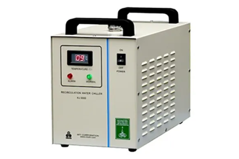
A laboratory chiller is a specially designed cooling system used to maintain a constant temperature for laboratory equipment or processes. The working principle is to circulate the cooling fluid (water, ethylene glycol or a specific refrigerant) in a closed-loop system, thereby removing the heat from the equipment or sample. This process ensures that the temperature remains stable and within the required range, which is crucial for the accuracy and reliability of many laboratory applications.
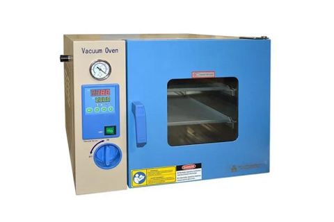
With the rapid development of modern industry, the importance of the product has gradually been reflected. This equipment is also widely used in industries such as pharmaceuticals, electronics and materials science. These industries also have high requirements for the drying and curing of sensitive materials. The Laboratory drying oven we produce fully meets the high demands of these industries and can help customers achieve high-performance production or experiments.


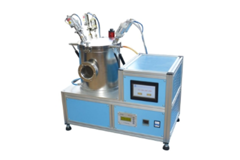
The emergence and application of sputtering technology has gone through many stages. After more than 30 years of development, magnetron sputtering technology has developed into an irreplaceable method for optical, electrical and other functional thin films.How much do you know about them?
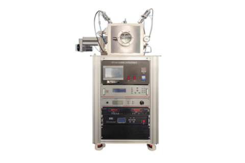
On the basis of basic magnetron sputtering,high vacuum and high temperature growth environment are introduced, and plasma technology is combined to improve the reaction efficiency of reactive deposition, so as to realize magnetron sputtering film epitaxy. The film prepared under this high vacuum condition has a better lattice orientation and more outstanding crystal properties. It has a wide range of applications in superconducting quantum, ferroelectric materials, piezoelectric materials, thermoelectric materials and other fields. The high vacuum state helps to reduce the influence of impurities and ensure that the sputtered particles do not react adversely with other gases during the deposition process.